- 您现在的位置:买卖IC网 > Sheet目录1216 > FR011L5J (Fairchild Semiconductor)LOW SIDE REV BIAS PROTECT 6MLP
�� �
�
�Absolute� Maximum� Ratings�
�Values� are� at� T� A� =25� °� C� unless� otherwise� noted.�
�Symbol�
�V+� MAX_OP�
�V+� 24�
�V-� MAX_OP�
�Parameter�
�Steady-State� Normal� Operating� Voltage� between� CTL� and� NEG� Pins�
�(V� IN� =� V+� MAX_OP� ,� I� IN� =� 1.5A,� Switch� On)�
�24-Hour� Normal� Operating� Voltage� Withstand� Capability� between� CTL� and�
�NEG� Pins� (V� IN� =� V+� 24� ,� I� IN� =� 1.5A,� Switch� On)�
�Steady-State� Reverse� Bias� Standoff� Voltage� between� CTL� and� NEG� Pins�
�(V� IN� =� V-� MAX_OP� )�
�Value�
�+20�
�+29�
�-30�
�Unit�
�V�
�V� IN� =� 5V,� Continuous�
�I� IN�
�Input� Current�
�(2)�
�(see� Figure� 4)�
�10�
�A�
�T� J�
�Operating� Junction� Temperature�
�150�
�°C�
�T� A� =� 25°C�
�(see� Figure� 5)�
�P� D�
�Power� Dissipation�
�T� A� =� 25°C� (2)� (see� Figure� 4)�
�(2)�
�2.4�
�0.9�
�W�
�I� DIODE_CONT� Steady-State� Diode� Continuous� Forward� Current� from� POS� to� NEG�
�I� DIODE_PULSE� Pulsed� Diode� Forward� Current� from� POS� to� NEG� (300μs� Pulse)�
�Human� Body� Model,� JESD22-A114�
�2�
�210�
�0.6�
�A�
�System� Model,� IEC61000-4-2�
�ESD�
�Electrostatic� Discharge�
�Capability�
�Charged� Device� Model,� JESD22-C101�
�Contact�
�(CTL� is� shorted� to� POS)� (3)� Air�
�2�
�8�
�15�
�kV�
�Notes:�
�1.� The� V� +24� rating� is� NOT� a� survival� guarantee.� It� is� a� statistically� calculated� survivability� reference� point� taken� on�
�qualification� devices,� where� the� predicted� failure� rate� is� less� than� 0.01%� at� the� specified� voltage� for� 24� hours.� It� is�
�intended� to� indicate� the� device’s� ability� to� withstand� transient� events� that� exceed� the� recommended� operating�
�voltage� rating.� Specification� is� based� on� qualification� devices� tested� using� accelerated� destructive� testing� at�
�higher� voltages,� as� well� as� production� pulse� testing� at� the� V� +24� level.� Production� device� field� life� results� may� vary.�
�Results� are� also� subject� to� variation� based� on� implementation,� environmental� considerations,� and� circuit�
�dynamics.� Systems� should� never� be� designed� with� the� intent� to� normally� operate� at� V� +24� levels.� Contact� Fairchild�
�Semiconductor� for� additional� information.�
�2.� The� device� power� dissipation� and� thermal� resistance� (R� θ� )� are� characterized� with� device� mounted� on� the� following�
�FR4� printed� circuit� boards,� as� shown� in� Figure� 4� and� Figure� 5�
�3.� Conducted� with� shorted� load.� Open� load� performance� is� not� guaranteed.�
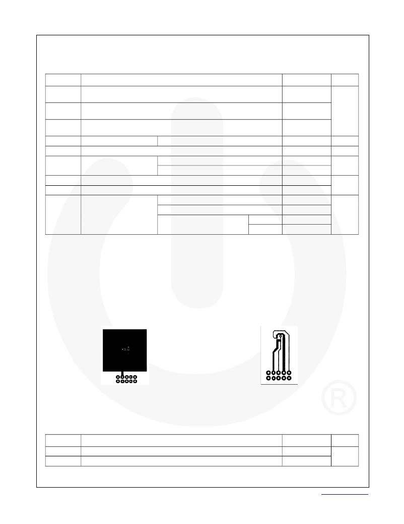
�Figure� 4.� 1� Square� Inch� of� 2-ounce� copper�
�Thermal� Characteristics�
�Figure� 5.� Minimum� Pads� of� 2-ounce� Copper�
�Symbol�
�Parameter�
�Value�
�Unit�
�Thermal� Resistance,� Junction� to� Ambient�
�Thermal� Resistance,� Junction� to� Ambient�
�R� θ� JA�
�R� θ� JA�
�(2)�
�(2)�
�(see� Figure� 4)�
�(see� Figure� 5)�
�61�
�153�
�°C/W�
�?� 2012� Fairchild� Semiconductor� Corporation�
�FR011L5J� ?� Rev.� C3�
�3�
�www.fairchildsemi.com�
�发布紧急采购,3分钟左右您将得到回复。
相关PDF资料
FR014H5JZ
HI SIDE REV BIAS PROTECT MLP
FR3-32M
EMULATOR MEMORY FLEXROM 3
FS-9062
JTAG_BOOSTER FOR ANALOG DEVICES
FS-977
JTAG-BOOSTER FOR 386EX 3.3V
FS1-R26-2000
CONN RECEPT MINI SAS 26POS SMD
FS1-R26-2001
CONN RECPT SAS MINI 26POS SMT
FS1-S01-146E1
CONN SNGL M-SAS CAGE KEY 4,6 P1
FS1-S02-1D66E1
CONN MINI SAS CAGE 1X2 R/A SMT
相关代理商/技术参数
FR014H5JZ
功能描述:TVS 二极管 - 瞬态电压抑制器 High-Side Reverse Bias Protector
RoHS:否 制造商:Vishay Semiconductors 极性:Bidirectional 工作电压: 击穿电压:58.9 V 钳位电压:77.4 V 峰值浪涌电流:38.8 A 系列: 封装 / 箱体:DO-214AB 最小工作温度:- 55 C 最大工作温度:+ 150 C
FR015L3EZ
功能描述:TVS 二极管 - 瞬态电压抑制器 LS Revrse Bias/Rvrse Polarity Protector RoHS:否 制造商:Vishay Semiconductors 极性:Bidirectional 工作电压: 击穿电压:58.9 V 钳位电压:77.4 V 峰值浪涌电流:38.8 A 系列: 封装 / 箱体:DO-214AB 最小工作温度:- 55 C 最大工作温度:+ 150 C
FR01AC10HB
制造商:NKK Switches 功能描述:DIP ROTARY
FR01AC10HB-S
功能描述:编码式波段开关 Series FR 10mm DIP Rotary Thru-hole
RoHS:否 制造商:C&K Components 位置数量:10 输出代码:Binary Coded Decimal 执行器:Screwdriver 触点额定值: 端接类型:Solder Pin 封装:Tube
FR01-AC10HB-ST
制造商:Nihon Dempa Kogyo Co (NDK) 功能描述:Switch,Rotary,Knob,PC-H Tab
FR01AC10H-S
制造商:NKK Switches 功能描述:DIP ROTARY
FR01AC10PB
功能描述:编码式波段开关 10mm DECIMAL YELLOW ACTUATOR
RoHS:否 制造商:C&K Components 位置数量:10 输出代码:Binary Coded Decimal 执行器:Screwdriver 触点额定值: 端接类型:Solder Pin 封装:Tube
FR01AC10PB-S
功能描述:编码式波段开关 10mm DECIMAL YELLOW ACTUATOR
RoHS:否 制造商:C&K Components 位置数量:10 输出代码:Binary Coded Decimal 执行器:Screwdriver 触点额定值: 端接类型:Solder Pin 封装:Tube